The problem
Nearly all public-key cryptography in use today rests on factoring large numbers (RSA) or the discrete logarithm over an elliptic curve (ECC), and Shor's algorithm removes the asymmetry both depend on once a large enough quantum computer exists. The threat does not wait for that hardware: traffic captured today can be stored until a machine exists that can open it, so anything with a long secrecy lifetime is already exposed. NIST's answer is ML-KEM, standardized in FIPS 203 and formerly known as CRYSTALS-Kyber. Its hardness comes from the Module Learning With Errors problem over polynomial rings with modulus 3329, believed to resist classical and quantum attacks alike.
ML-KEM was designed to be practical on a general-purpose CPU, and it is. That is a different question from whether it should run there. A data center terminating TLS performs key encapsulation constantly, and full adoption of the standard turns that into an enormous aggregate workload. Two operations dominate the cost: the Number-Theoretic Transform, which moves polynomials into a representation where multiplication is cheap, and the Keccak permutation inside the SHAKE hash functions, which expands a 32-byte seed into the public matrix. The NTT unrolls into layers of independent butterfly operations, and independence is exactly the property that makes a workload worth putting on an FPGA.
Two tracks, measured against each other
The accelerator side started from BSC LOCA's open-source Vitis HLS design rather than RTL of our own, synthesized under Vitis 2023.1 for part xcu280-fsvh2892-2L-e at a 300 MHz target clock. Cycle latency came from a full C/RTL co-simulation rather than a complete Vivado implementation. Driving the real implementation means wrapping the AXI interfaces and supplying clock and reset from a host design, and a first attempt without that wrapper asked for more than 2,000 I/O pins, which no real part provides. Since the comparison is cycles, resources, and power rather than board-level throughput, co-simulation gave the accuracy we needed and left enough time to try different HLS configurations.
The software side used the PQClean implementation of ML-KEM-512, chosen because it is a
clean, widely used reference. We wrote a testbench that runs KeyGen, Encap, and Decap in
series inside a marked region of interest, so the numbers cover the cryptography and nothing
around it. That ran under Sniper 7.3 on two configurations: gainestown, a
2.66 GHz out-of-order Nehalem-class core, and silvermont, a 1 GHz
in-order Atom-class core. Ten trials each, to catch run-to-run variance. I built and ran that
software side myself, from the PQClean testbench through both Sniper configurations, and
implemented both of the optimization experiments further down this page.
Both sides being simulated is a feature of the comparison, not a compromise in it. No thermal throttling, no OS scheduler, no background load, and neither side gets an advantage the other lacks. The absolute numbers would move on real silicon; the ratio between them is cleaner this way.
One asymmetry we had to state rather than hide: the HLS design exposes no separate KeyGen kernel. The expensive pieces of key generation, matrix expansion and centered-binomial sampling, happen inside Encapsulate, so its hardware cost is counted, but a KeyGen-to-KeyGen comparison does not exist. Totals still compare.
What the numbers said
Cycle counts flatter the FPGA, which runs at 300 MHz against 2.66 GHz, so the honest number is wall-clock time. On that measure the accelerator finishes 11 times sooner than the out-of-order core and 43 times sooner than the in-order one.
| Measure | ML-KEM accelerator | Gainestown, out-of-order | Silvermont, in-order |
|---|---|---|---|
| Cycles | 11,948 | 1,195,000 | 1,724,000 |
| Wall-clock time | 0.0398 ms | 0.448 ms | 1.724 ms |
| Average power | 11.09 W | 20.15 W | 6.56 W |
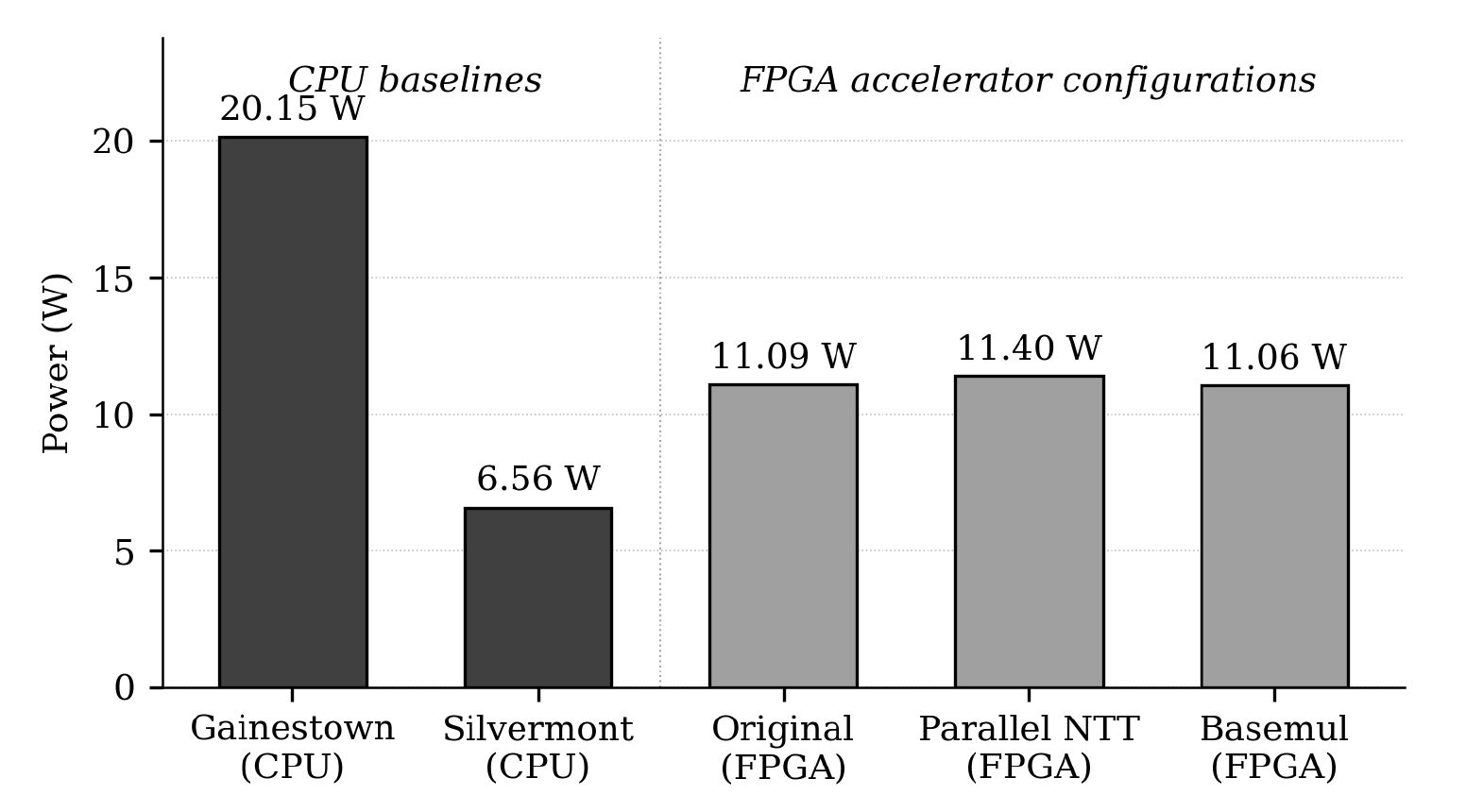
Beating a fast core on both time and power is the result that matters for the data-center case; losing to the low-power in-order core on watts while finishing 43 times sooner is a trade most operators would take. Thermal and environmental parameters came from Vivado's U280 data, with heat sink and airflow set to what a rack deployment would look like.
The resource report is what set up the rest of the project. The design fits in 13% of the U280's LUTs, 3% of its DSPs, and 1% of its block RAM. Most of the chip sits unused, which is an invitation to spend it.
Two optimizations, one halved and neither faster
The obvious lever was unrolling, and the reference design had already pulled it. The NTT and
inverse NTT layers and their inner butterfly loops were unrolled about as far as they go.
What was left was the module rank K, the parameter that sets the security level.
ML-KEM-512 uses K=2, so two polynomials run through the NTT sequentially. We duplicated the
module inside NTT_Layer and called it once per polynomial, which cut per-layer
latency from 521 cycles to 265, a 49% reduction. The same approach extends to K=3 and K=4 for
the higher security levels, at the cost of the parameterized modularity we gave up.
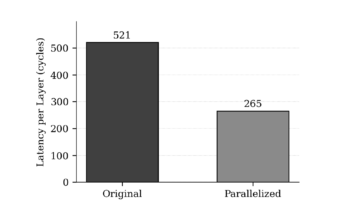
Total cycles for the full pipeline went from 11,948 to 11,967. Halving a stage bought nothing at all, and the resource cost was real: 21% more BRAM, 23% more DSPs, 10% more LUTs, plus a 2.8% increase in power. Whatever the NTT was waiting on, it was still waiting on it.
So the NTT was not on the critical path. Finding what was took reading the design, because
the synthesis report does not label which stages run concurrently in a dataflow region. Going
through the code alongside the per-stage latencies and initiation intervals pointed at
Readmem, Split, basemul_montgomery, and basemul_add. The two basemul
modules handle coefficient-wise multiplication in the NTT domain across 128 to 256
coefficients. Widening their buffers to move four coefficients per pass instead of one should
have raised throughput.
It did not move the cycle counts either: 529 to 528 on basemul_montgomery, and
515 to 515 on basemul_add. The resource numbers confirm the architecture
genuinely changed, with flip-flop usage on basemul_add going from 69 to 232, so
the hardware is different and the schedule is not. The likeliest explanation is data
starvation. Widening two modules accomplishes little when most of the ports feeding them
still carry one coefficient at a time, which means the buffers would have to be widened
through the whole design rather than at the modules that looked slowest. Confirming that
needs a co-simulation of the widened build, and that run exhausted the RAM on the machines we
had. It stays an unproven hypothesis rather than a conclusion.
The other find was a bug in the reference design: the AXI master port bundles had no stream depths specified. We set them manually to get data flowing at all. Synthesis and implementation take about two hours per configuration, which put a hard ceiling on how many variants we could try, and experimenting with those stream depths never made the cut.
What I took away
A faster block is not a faster program. I knew that as a formula before this project, but watching a 49% latency reduction produce a 0.16% change in total cycles is a different kind of knowing. The interesting part was that Amdahl's law was the wrong explanation. The NTT is not a small fraction of the work; it was already fast enough that something else in the dataflow architecture set the pace, and no amount of improvement there was going to show up at the top.
Most of the real skill turned out to be reading a design nobody on the team wrote. The tools report latency and resource usage per module and leave the causal structure to you, so locating a bottleneck meant cross-referencing initiation intervals against the code and forming a hypothesis that could be wrong. Ours was wrong twice.
A two-hour build loop changes how you plan, too. Batching configurations and deciding what a run would prove before starting it beats iterating by feel.
Neither optimization worked, and the paper says so. That was the most useful part to write.
Credits & sources
- Co-author: Patrick Johnson (Tufts University). The design, benchmarking, and analysis were joint work throughout.
- Accelerator source: BSC LOCA, PQC-Crystals-HLS-Accelerators, GitHub repository, 2024. The accelerator is their open-source design and we did not write the bulk of that code. Our work was building and co-simulating it for our target, measuring it against CPU baselines, and attempting two optimizations on top of it.
- CPU baseline source: The PQClean Project, portable implementations of post-quantum cryptography.
- Standard: NIST, Module-Lattice-Based Key-Encapsulation Mechanism Standard, FIPS 203 (Final), August 2024.
Figures are taken from our own paper, linked at the top of this page.